

Beyond Fabs: Building India’s Semiconductor Ecosystem
引用元:EE Times India
日 付:2026年9月3日
著 者:井原 康孝(田中貴金属工業株式会社 取締役執行役員)
リンク:Beyond Fabs: Building India’s Semiconductor Ecosystem
インドで進む半導体産業の立ち上げは、製造能力だけでなく、バリューチェーン全体にわたる材料の知見、エンジニアリング能力、そして技術パートナーシップへの需要をも生み出している。
インドの半導体構想は、政策の発表段階から実際の製造へと急速に歩を進めている。新設のファブ、パッケージング拠点、エレクトロニクスクラスター、設計関連の取り組みが、国内半導体産業の基盤を形づくり始めた。
しかし、世界で戦えるエコシステムを築くには、製造能力だけでは足りない。より難しいのは、それらの拠点を安定的に、かつ量産規模で稼働させるために必要な材料、プロセスエンジニアリング、製造ノウハウ、そして技術人材を育てることである。各プロジェクトが開発・材料認定の段階から量産へと移るにつれ、材料品質の均一性とプロセスの信頼性はいっそう重みを増していく。
ここに、経験を積んだ技術サプライヤーが果たしうる役割がある。インドの産業が初期投資と認定の段階から量産へ移行していく局面では、なおさらである。
田中貴金属にとって、インドの半導体分野の拡大は、いくつかの潮流が重なって生まれた長期的な機会である。同国のエレクトロニクス市場の成長は、自動車、産業用エレクトロニクス、コンシューマー機器、通信、AI、デジタルインフラといった幅広い領域で需要を生み出している。同時に、豊富なエンジニアリング人材と拡大する産業基盤が、より広い半導体エコシステムの形成を後押ししている。
田中貴金属は2019年にムンバイ拠点を設けて以来、インドでの活動を続けてきた。これが、同国で発展を続ける半導体・エレクトロニクス・自動車の各産業と、より緊密に関わるための足がかりとなっている。
もう一つ心強いのは、インドの半導体産業が製造能力だけにとどまらず、裾野を広げ続けている点だ。先端パッケージング、半導体検査(テスト)、設計、そしてそれらを支えるサプライチェーンへの投資が増えており、長期的な産業成長の土台が築かれつつある。
この広がりには大きな意味がある。半導体製造は、単独の工程として完結するものではないからだ。ファブやパッケージング工場は、厳密に管理された材料、装置、プロセス技術、そして技術サポートを供給できるサプライヤーのネットワークに支えられて、はじめて成り立つ。
「インドの半導体産業が開発・認定の段階から量産へと移行していく中で、認定された材料を選び、堅牢な製造プロセスを確立することの重要性は、いっそう高まっていく」と、田中貴金属工業株式会社 取締役執行役員の井原康孝は語る。「世界の半導体メーカーを支えてきた数十年の経験を踏まえ、インドの製造能力が育っていく過程で、材料とアプリケーションの知見を提供できると考えている」
先端パッケージングが早期の成長領域になりうる
インドで立ち上がりつつある半導体バリューチェーンの中でも、先端パッケージングと半導体検査は、比較的早い段階で機会が生まれる領域といえる。
これは、他の新興半導体市場でも見られてきたパターンだ。前工程を含む広範な製造エコシステムが成熟するより先に、パッケージングと検査の能力が整い、スケールしていく。
田中貴金属の見方でも、近い将来の最大の機会は先端パッケージングと半導体検査にある。多くの新興半導体市場で実際に観察してきた発展の道筋である。
先端パッケージングは、材料への要求も厳しくしている。電力密度の上昇、より小さなフォームファクター、より高い配線密度は、製品の稼働期間を通じて電気的・機械的・熱的な性能を保ち続ける材料を必要とする。
ヘテロジニアスインテグレーションは、より多くの機能とインターフェースをパッケージ内に取り込むことで、この複雑さをさらに押し上げる。接合界面、材料の適合性、プロセス制御への要求は高まり、それはパッケージの信頼性と製造歩留まりに直結する。
材料サプライヤーにとってこれは、量産が始まってから参入するのではなく、顧客の認定作業やプロセス開発の初期段階から関与できる機会でもある。
田中貴金属としても、認定から量産立ち上げにかけての期間に顧客を支えることこそ、最も貢献できる場面だと考えている。
技術の進化とともに重要性を増す貴金属材料
インドの半導体能力がパッケージングと検査からウエハー製造へと広がるにつれ、材料への要求はさらに専門的になっていく。
貴金属は、半導体産業の黎明期から製造を支えてきた。工程やアプリケーションが求める電気的・熱的・化学的・機械的な特性に応じて、さまざまな貴金属とその合金が選ばれている。

金(Au)ボンディングワイヤは、半導体パッケージングにおける貴金属活用の最も初期の例の一つであり、田中貴金属の関与は1960年代にさかのぼる。ワイヤボンディングは成熟した技術だが、その要求はデバイスの微細化、パッケージ設計の変化、信頼性への期待の高まりとともに進化を続けている。それが、ワイヤの組成、機械的特性、ファインピッチ対応、ボンディング性能の継続的な開発を促してきた。田中貴金属は顧客と緊密に連携し、デバイスやプロセスごとの要求に合わせてボンディング材料を開発・最適化している。
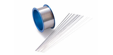
現在、田中貴金属は半導体の相互接続向けに、細線・極細線の金(Au)、銀(Ag)合金、銅(Cu)、パラジウム被覆銅(PCC)の各ボンディングワイヤを供給しており、細線の線径はおおむね14〜80µmである。パワーデバイス向けには、より太いアルミニウム(Al)線・銅(Cu)線やリボンを取り揃え、線径は100〜500µmに及ぶ。材料の選定は、用途と、電気特性・ボンダビリティ・機械的特性・信頼性のどのバランスを求めるかによって決まる。安定したボンディングには表面品質と寸法安定性の作り込みも欠かせず、そこでは金属接合に関する知見が生きている。
ダイアタッチは、とりわけパワー半導体において別種の課題を突きつける。基板との接合の信頼性を保ちながら、ダイから効率よく熱を逃がさなければならない。銀接着剤は、Siはもちろん、熱性能と接合部の長期信頼性が重視されるSiCやGaNといったワイドバンドギャップ半導体デバイスに対しても、一つの解となる。

半導体検査は、材料に電気的・機械的な要求を同時に課す。プローブピンは、摩耗に耐えながら電気的接触を繰り返し確立しなければならない。たとえばパラジウム合金のプローブピン材料は、電気的な機能に硬さと耐摩耗性を併せ持つ。検査ピッチが微細になるほど、こうした特性の重要性は増していく。
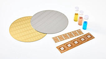
さらに上流のウエハー製造では、薄膜プロセス向けに厳密に管理された材料が求められる。高純度スパッタリングターゲット、貴金属めっき液、CVD/ALD用プリカーサーは、それぞれ異なる工程要求に応えるものであり、いずれも材料の純度・組成・均一性の管理が、安定した製造を左右する。
重要なのは個々の材料そのものというより、適切な材料特性を選び取り、それを製造プロセスに確実に組み込むことである。
田中貴金属の強みは、先端貴金属材料、材料エンジニアリング、アプリケーションサポートを組み合わせ、ウエハー製造から先端パッケージング、検査に至る半導体製造フロー全体で顧客を支えられる点にある。
このことは、インドの半導体産業がAI、自動車の電動化、パワーエレクトロニクスを牽引役とする技術領域を狙ううえで、とりわけ意味を持つ。
AIアクセラレータはパッケージングと熱性能への要求を高め、電気自動車や産業システムはSiC・GaNなどを用いたパワー半導体の採用を加速させている。
演算性能の向上、電力密度の上昇、動作温度の高温化、製品寿命の長期化。いずれも、製造の安定性を保ちながら、電気・熱・信頼性の面でより厳しい要求を満たす材料を必要とする。
材料そのものは目新しいものではないかもしれない。しかし半導体技術は、前工程での高純度化と精密な組成制御から、パッケージングと検査における電気的・熱的・機械的性能まで、材料に課す要求を上げ続けている。
エンジニアリング人材という戦略資産
材料だけで半導体産業は生まれない。
インドには厚いエンジニアリング人材の層があり、インドのエンジニアは世界の半導体開発に貢献してきた。国内の半導体製造が拡大するいま、その専門性をより多く製造とプロセスエンジニアリングに振り向けることが、産業の継続的な発展を後押しする。
半導体製造には、プロセスインテグレーション、歩留まり、信頼性、材料、装置、そして大量生産を理解する専門人材が必要だ。
さらに、製造現場の判断力、すなわちプロセスのばらつきを診断し、材料や装置を認定し、歩留まりを継続的に改善していく力を育てるには、時間がかかる。
製造能力の立ち上げ期、とりわけ材料認定、プロセス開発、量産への移行という局面で技術パートナーシップが大きな意味を持つのは、このためである。
サプライヤーから技術パートナーへ
半導体産業の複雑さゆえに、あらゆる能力を一社だけで内製することは難しい。半導体産業が確立した地域では、メーカー、装置サプライヤー、材料メーカー、研究機関、大学が緊密に結び付いたエコシステムが築かれてきた。
インドもまた、製造基盤が成熟していく過程で同じような関係を必要とするだろう。
田中貴金属は、材料認定、アプリケーションサポート、技術協業を通じて、要求の変化に合わせながら半導体メーカーと緊密に取り組んでいく方針である。あわせて研究機関や業界団体との連携にも機会を見出しており、グローバルな供給網を生かして、半導体材料と技術サポートへの確実なアクセスを顧客に提供していく。
競争力ある半導体産業を築くには、バリューチェーン全体での連携が要る。中心にいるのはメーカーだが、研究機関、業界団体、技術コンソーシアムもまた、能力構築と技術開発に貢献しうる。
こうした交流は、顧客が材料認定から安定生産へと進んでいく中で、材料サプライヤーがアプリケーションとプロセスの要求をより深く理解する助けにもなる。
サプライチェーンの強靭性は材料にも及ぶ
安定した半導体生産を支えるのは、製造能力だけではない。均一な材料品質、確実な調達、そして認定されたサプライヤーの存在が欠かせない。田中貴金属の140年を超える貴金属事業の歩みは、調達から精製、材料製造までを網羅しており、貴金属のライフサイクル全体にわたる知見を蓄えてきた。
リサイクルもまた、このライフサイクルの一部である。貴金属は回収・精製して再び使うことができる。調達、材料製造、回収、精製を組み合わせることで、より循環型に近い材料の流れをつくることができる。これは貴重な資源の効率的な活用につながると同時に、長期的な材料供給を支えることにもなる。
今後5年は「能力構築」の時代
インドはすでに、半導体産業を成長させるための要素の多くをそろえている。政府の支援、大きなエレクトロニクス市場、エンジニアリング人材、そしてグローバルなテクノロジー企業の参画の広がりである。
次の段階は、より難しい。
投資を確実な生産に変え、国内の技術的専門性を育て、認定されたサプライヤー網を築き、成熟した半導体地域と競うために必要な製造知識を確立しなければならない。
だからこそ、長期的な技術パートナーシップが重要になる。
田中貴金属にとっての成功とは、顧客が信頼性の高い、高品質な半導体製造を築いていくのを支えることである。それは、材料認定、プロセス開発、そして先端パッケージングと半導体検査、さらにエコシステムの成熟に伴うウエハー製造における実証済み技術の導入を通じて実現される。
前工程材料から先端パッケージング、半導体検査まで長年積み重ねてきた経験は、インドの製造要求が高度化していく中で顧客を支える土台となる。
インドの半導体構想から引き出せる教訓は、シンプルだ。ファブは生産能力を生むが、競争力を生むのはエコシステムである。
工場は目に見える土台を用意する。しかし、材料科学、プロセスの専門性、エンジニアリング人材、サプライヤーとの関係、そして何十年もかけて蓄積された製造知識という、目に見えにくい層こそが、インドが半導体の野心を持続させ、スケールさせられるかどうかを決めることになる。
これらの層にまたがる経験を持つ技術パートナーにとって、インドの成長は単なる新市場以上の意味を持つ。それは、同国の半導体産業が最終的に競い合っていくための技術的な土台づくりに、ともに携わる機会なのである。
SEMICON India 2026に出展
田中貴金属は「SEMICON India 2026」(2026年9月17日〜19日、インド・ニューデリー Yashobhoomi)に出展する。前工程、パッケージング、検査の各工程、そして貴金属リサイクルまで、半導体産業を支える貴金属材料と関連技術を幅広く紹介する予定である。
ブース(Booth No. H4 218)では技術スペシャリストが直接対応する。材料に関する課題、アプリケーション要求、協業の可能性について、ぜひ気軽に相談いただきたい。
※編集者注:貴金属とは、金(Au)、銀(Ag)、白金(Pt)、パラジウム(Pd)、イリジウム(Ir)、ロジウム(Rh)、ルテニウム(Ru)、オスミウム(Os)の8元素を指す。
【記事引用元】Beyond Fabs: Building India's Semiconductor Ecosystem
関連情報

Source: EE Times India
Date: September 3, 2026
Author: Yasutaka Ihara (Director & Corporate Officer, TANAKA PRECIOUS METAL TECHNOLOGIES Co., Ltd.)
Link: Beyond Fabs: Building India’s Semiconductor Ecosystem
India's semiconductor build-out is creating demand not only for manufacturing capacity, but also for materials expertise, engineering capabilities and technology partnerships across the value chain.
India's semiconductor ambitions have moved rapidly from policy announcements toward physical manufacturing. New fabs, packaging facilities, electronics clusters and design initiatives are beginning to establish the foundations of a domestic semiconductor industry.
But building a globally competitive ecosystem will require more than manufacturing capacity. The harder task is developing the materials, process engineering, manufacturing know-how and technical talent needed to operate those facilities reliably and at scale. As projects move from development and material qualification toward volume production, consistency in material quality and process reliability becomes increasingly important.
This is where experienced technology suppliers can play an important role, particularly as India's industry moves from initial investments and qualification toward volume production.
For TANAKA, India's semiconductor expansion represents a long-term opportunity shaped by several converging trends. The country's growing electronics market is creating demand across automotive, industrial electronics, consumer devices, telecommunications, AI and digital infrastructure, while its engineering talent and expanding industrial base are supporting the development of a broader semiconductor ecosystem.
TANAKA has maintained a presence in India since establishing its Mumbai base in 2019, providing a foundation for closer engagement with the country's developing semiconductor, electronics and automotive industries.
Another encouraging development is the continued expansion of India's semiconductor industry beyond manufacturing capacity alone. Increasing investment across advanced packaging, semiconductor testing, design, and the supporting supply chain is laying the foundation for long-term industry growth.
That broader development is significant. Semiconductor manufacturing does not operate as an isolated process. A fab or packaging plant depends on a network of suppliers capable of delivering highly controlled materials, equipment, process technologies and technical support.
"As India's semiconductor industry moves from development and qualification toward volume production, selecting qualified materials and establishing robust manufacturing processes will become increasingly important," says Yasutaka Ihara, Director & Corporate Officer at TANAKA PRECIOUS METAL TECHNOLOGIES Co., Ltd. "Drawing on decades of experience supporting semiconductor manufacturers globally, we see an opportunity to contribute materials and application expertise as India's manufacturing capabilities develop."
Advanced packaging may be an early growth area
Among the different parts of India's emerging semiconductor value chain, advanced packaging and semiconductor testing could offer some of the most immediate opportunities.
This reflects a pattern seen in other emerging semiconductor markets, where packaging and testing capabilities can be established and scaled before a broader front-end manufacturing ecosystem reaches maturity.
From our perspective, the greatest near-term opportunities lie in advanced packaging and semiconductor testing. This is a development path we have observed in many emerging semiconductor markets.
Advanced packaging also introduces increasingly demanding requirements for materials. Higher power densities, smaller form factors, and greater interconnect density require materials that can maintain electrical, mechanical, and thermal performance throughout the product's operating life.
Heterogeneous integration adds to this complexity by bringing more functions and interfaces into the package. This places greater demands on bonding interfaces, material compatibility and process control, with implications for package reliability and manufacturing yield.
For materials suppliers, this creates opportunities to become involved early in customer qualification and process development rather than entering only after manufacturing has reached volume.
For TANAKA, supporting customers during qualification and manufacturing ramp-up is where we believe we can make the greatest contribution.
Precious metal materials become more critical as technology advances
As India's semiconductor capabilities expand from packaging and testing into wafer fabrication, the materials requirements will become even more specialized.
Precious metals have supported semiconductor manufacturing since the industry's early development. Different precious metals and their alloys are selected according to the electrical, thermal, chemical, and mechanical characteristics required by a particular process or application.
Gold (Au) bonding wire is one of the earliest examples of precious metals in semiconductor packaging, with TANAKA's involvement dating back to the 1960s. Although wire bonding is a mature technology, its requirements continue to evolve with device scaling, changing package designs, and higher reliability expectations. This drives ongoing development in wire composition, mechanical properties, fine-pitch capability, and bonding performance. Working closely with customers, TANAKA develops and optimizes bonding materials for specific device and process requirements.
Today, TANAKA provides fine and ultra-fine Au, silver (Ag)-alloy, copper (Cu) and palladium (Pd)-coated Cu (PCC) bonding wires for semiconductor interconnections, with fine-wire diameters typically ranging from 14 to 80 µm. For power-device applications, thicker Aluminum (Al) and Cu wires and ribbons are available, with wire diameters ranging from 100 to 500 µm. Material selection depends on the application and the required balance of electrical performance, bondability, mechanical properties, and reliability. Controlled surface quality and dimensional stability are also important for consistent bonding, supported by expertise in metal bonding.
Die attach presents a different challenge, particularly for power semiconductors. Heat must be transferred efficiently from the die while maintaining a reliable bond with the substrate. Ag adhesive paste provides one approach for Si as well as wide-bandgap semiconductor devices based on SiC and GaN, where thermal performance and long-term joint reliability are important.
Semiconductor testing places both electrical and mechanical demands on materials. Probe pins must repeatedly establish electrical contact while resisting wear. Palladium-alloy probe pin materials, for example, combine electrical functionality with hardness and wear resistance, characteristics that become increasingly important as test pitches become finer.
Further upstream, wafer fabrication requires highly controlled materials for thin-film processes. High-purity sputtering targets, precious-metal plating solutions, and CVD/ALD precursors serve different process requirements, where control of material purity, composition and consistency is important for stable manufacturing.
The significance is less about any individual material than selecting the appropriate material properties and integrating them reliably into the manufacturing process.
What differentiates TANAKA is our ability to support customers across the entire semiconductor manufacturing flow—from wafer fabrication and advanced packaging to testing—through a combination of advanced precious metal materials, materials engineering, and application support.
This becomes particularly relevant as India's semiconductor industry targets technologies driven by AI, automotive electrification and power electronics.
AI accelerators are increasing demands on packaging and thermal performance, while electric vehicles and industrial systems are accelerating adoption of power semiconductors based on technologies such as SiC and GaN.
Higher computing performance, greater power density, higher operating temperatures, and longer product lifetimes require materials that meet increasingly demanding electrical, thermal and reliability requirements while maintaining manufacturing consistency.
The materials themselves may be familiar, but semiconductor technology continues to raise the requirements placed on them—from high purity and precise composition control in front-end processes to increasingly demanding electrical, thermal and mechanical performance in packaging and testing.
Engineering talent is a strategic asset
Materials alone cannot create a semiconductor industry.
India has a substantial engineering talent base, with Indian engineers contributing to semiconductor development globally. As domestic semiconductor manufacturing expands, applying more of this expertise to manufacturing and process engineering can support the industry's continued development.
Semiconductor manufacturing needs specialists who understand process integration, yield, reliability, materials, equipment, and high-volume production.
It also takes time to develop manufacturing judgment—the ability to diagnose process variation, qualify materials and equipment, and continuously improve yield.
This is one reason technical partnerships can be particularly valuable as manufacturing capabilities develop, particularly during material qualification, process development and the transition to volume production.
From suppliers to technology partners
The semiconductor industry's complexity makes it difficult for any single company to develop every capability internally. Established semiconductor regions have built ecosystems around close relationships between manufacturers, equipment suppliers, materials companies, research institutions and universities.
India will need similar relationships as its manufacturing base matures.
TANAKA's approach is to work closely with semiconductor manufacturers as their requirements evolve, particularly through material qualification, application support, and technical collaboration. At the same time, TANAKA sees opportunities to engage with research institutes and industry organizations, while drawing on its global supply network to provide customers with reliable access to semiconductor materials and technical support.
Building a competitive semiconductor industry requires coordination across the value chain. While manufacturers are central to this development, research institutions, industry organizations and technical consortiums can also contribute to capability building and technology development.
This interaction can also help materials suppliers better understand application and process requirements as customers move from material qualification toward stable production.
Supply-chain resilience includes materials
Reliable semiconductor production depends not only on manufacturing capacity, but also on consistent material quality, dependable procurement, and qualified suppliers. TANAKA's more than 140 years of experience in precious metals spans procurement, refining and materials manufacturing, providing expertise across the precious metal lifecycle.
Recycling is also part of this lifecycle. Precious metals can be recovered and refined for reuse, and combining procurement, materials manufacturing, recovery and refining can create a more circular materials loop. This helps make efficient use of valuable resources while supporting longer-term material supply.
The next five years will be about capability building
India has already established many of the ingredients needed for semiconductor growth: government support, a large electronics market, engineering talent and increasing participation from global technology companies.
The next stage is more difficult.
The country must turn investment into reliable production, develop local technical expertise, build qualified supplier networks, and establish the manufacturing knowledge required to compete with mature semiconductor regions.
That makes long-term technology partnerships particularly important.
For TANAKA, success means supporting customers as they build reliable, high-quality semiconductor manufacturing, including through material qualification, process development and the adoption of proven technologies across advanced packaging, semiconductor testing and, as the ecosystem matures, wafer fabrication.
TANAKA's long-standing experience across front-end materials, advanced packaging and semiconductor testing provides a foundation for supporting customers as India's manufacturing requirements become more sophisticated.
The broader lesson for India's semiconductor ambitions is straightforward: fabs create capacity, but ecosystems create competitiveness.
Manufacturing plants may provide the visible foundation, but the less visible layers—materials science, process expertise, engineering talent, supplier relationships and decades of accumulated manufacturing knowledge—will determine whether India can sustain and scale its semiconductor ambitions.
For technology partners with experience across these layers, India's growth therefore represents more than a new market. It is an opportunity to help build the technical foundation on which the country's semiconductor industry will ultimately compete.
Exhibiting at SEMICON India 2026
TANAKA will be exhibiting at SEMICON India 2026 (Sept 17–19, Yashobhoomi, New Delhi, India), where it will showcase its comprehensive range of precious metal materials and related technologies supporting the semiconductor industry across front-end, packaging, testing processes, and precious metal recycling.
Please do visit the TANAKA booth [Booth No. H4 218] to engage directly with technical specialists and explore opportunities for deeper discussion on material challenges, application requirements, and potential collaboration.
Editorial note: Precious metals comprise eight metallic elements: silver (Ag), gold (Au), platinum (Pt), palladium (Pd), iridium (Ir), rhodium (Rh), ruthenium (Ru) and osmium (Os).
[Source] Beyond Fabs: Building India's Semiconductor Ecosystem
Related information
這篇報道怎麽樣?
請參考的人分享。


