

Probe Pin Materials
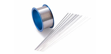
What is "Probe Pin Material"?
These micro-contact parts are used in electrical property testing (wafer testing and final testing) of semiconductors and electronic components, and require high contact stability and durability. TANAKA uses its own proprietary high-performance precious metal alloys, such as Pd-Ag-Cu, Pd-Ag-Au-Pt-Cu, and high-hardness Pd alloys, and offers wires in sizes from Φ20 to 1,000µm, as well as Pd-Ag-Cu and Cu alloy sheet materials.
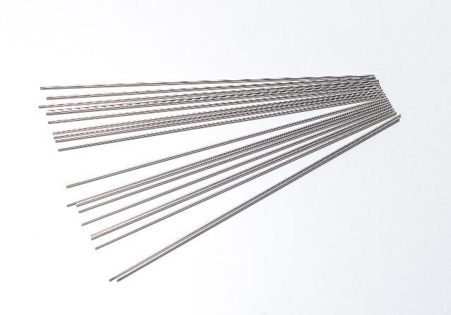
Precious metal-based Probe Pin material used in the inspection process of semiconductor manufacturing.
We offer a wide range of precious metal materials for probe pins used in inspections carried out during the front-end and back-end of semiconductor manufacturing.
Uses of Probe Pin Materials
Electrical tests are conducted on semiconductor integrated circuits during both the front-end and back-end of the manufacturing process.
The electrical test conducted during the front-end is called wafer testing, and probe cards are used. Probe pins of cantilever-type or vertical-type are used as probes on probe cards.
The electrical test conducted during the back-end is called final testing, and test sockets are used. Spring Probe ※ probe pins are used as probes on test sockets.
The required performance of Probe Pin materials varies depending on their intended use, including mechanical properties such as hardness and bendability and electrical properties such as electrical resistivity, so various materials are available.
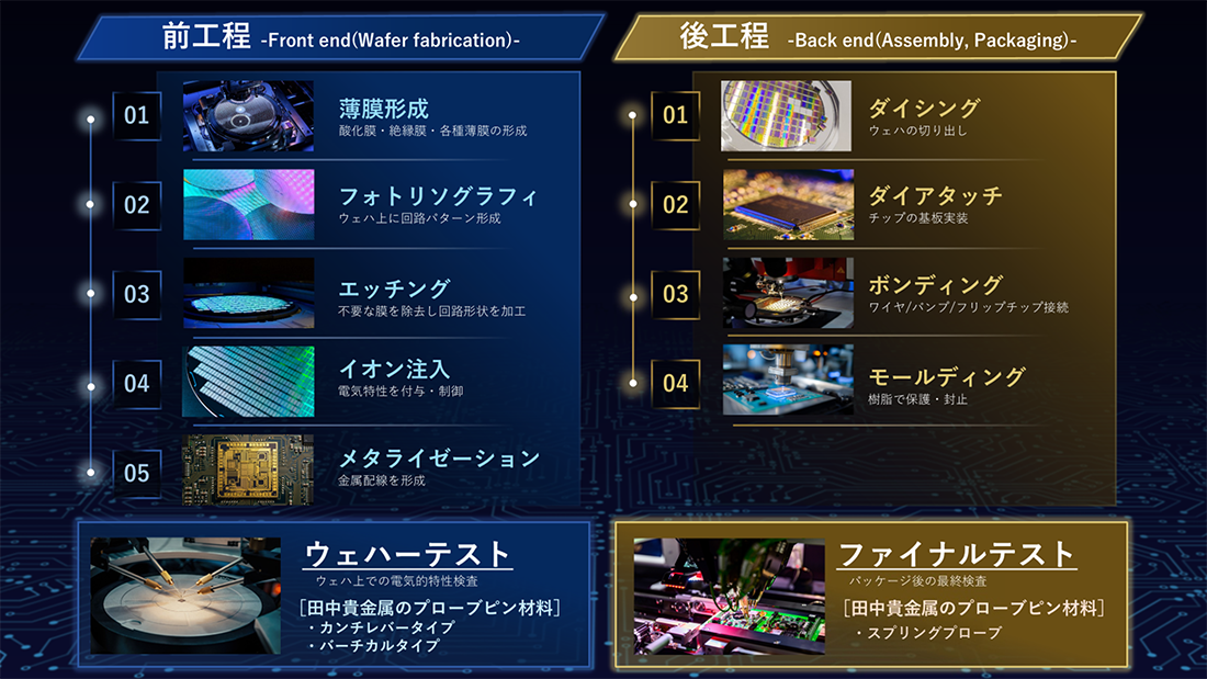
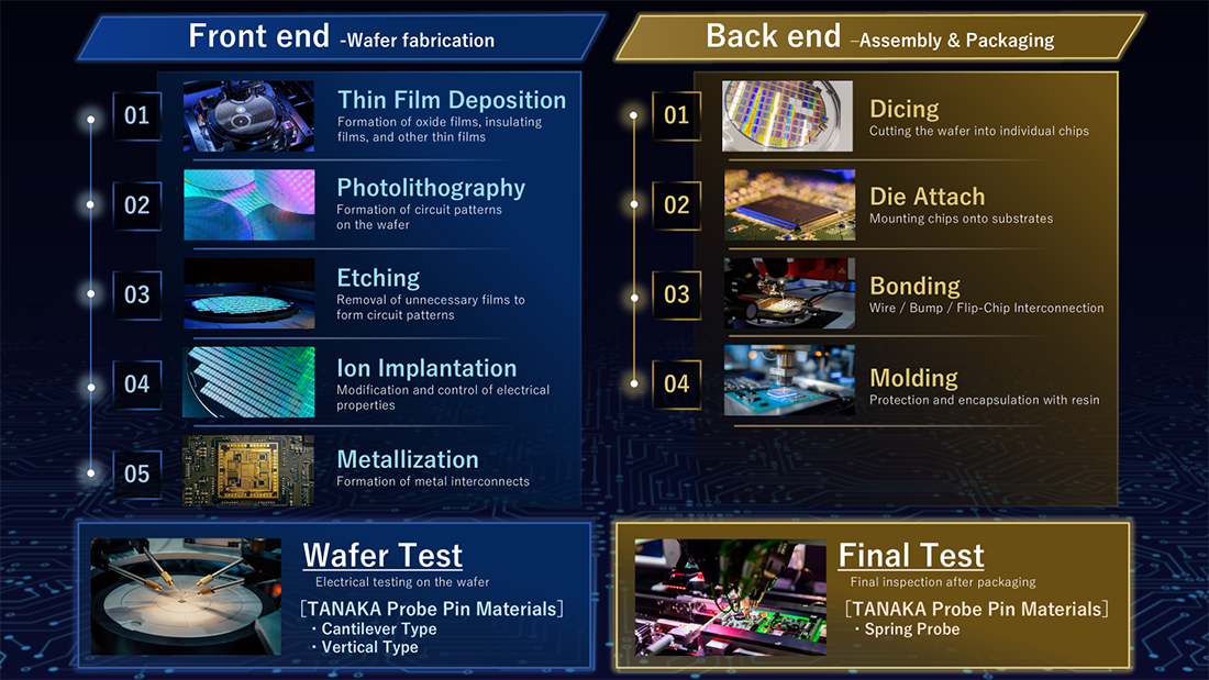
※ Spring probe is commonly referred to as pogo pin. “POGO” is a registered trademark of Everett Charles Technologies, Inc.
Types and Features of Probe Pins
Cantilever-type
- Features: Used in probe cards with terminal structures that operate on the principle of a cantilever beam. The tip of the Probe Pin is subjected to tapering and bending to form a needle shape.
- Material requirements: Material hardness, linearity, electrical resistivity, bendability, etc.
- Wire diameter: Φ50 to 300µm
Vertical-type
- Features: Used in probe cards with a terminal structure that arranges probes in the vertical direction, and depending on the method, buckling deformation may be used. The tip of the Probe Pin is processed into a needle or hemispherical shape according to the electrode shape of the device under test.
- Material requirements: Material hardness, linearity, electrical resistivity, bendability, etc.
- Wire diameter: Φ20 to 70µm
Spring Probe
- Features: Also called contact probe. It is used for electrical continuity testing of ICs, electronic components, and printed circuit boards. The tip is shaped according to the object being tested.
- Material requirements: Material hardness, linearity, contact resistance, etc.
- Wire diameter: Φ500µm to 1,000µm
Major Materials for Probe Pins
| SP-1 | SP-2 | TK-1Pro | TK-FS | TK-SK | TK-SR | Ir | ||
|---|---|---|---|---|---|---|---|---|
| Composition (mass%) |
Pd | 35 | – | 40 | 55.8 | 48.9 | – | – |
| Ag | 30 | 10 | 29.5 | 6.9 | 19.25 | – | – | |
| Au | 10 | 70 | – | – | – | – | – | |
| Pt | 10 | 5 | – | – | – | – | – | |
| Others | Cu, Zn | Cu, Ni | Cu, etc. | Cu, etc. | Cu, etc. | Rh | Ir | |
| Wire diameter range (mm) | 0.08-1.00 | 0.08-1.00 | 0.1-1.00 | 0.03-1.00 | 0.50-0.8 | 0.018-0.30 | 0.03-0.30 | |
| Electrical resistivity |
25-33 | 13.3 | 11 | 6.1-6.9 | 16.1 | 5.3-7.0 | 5.6 | |
| Electrical conductivity (%IACS) | 5.2-6.9 | 13 | 15.7 | 25.0-28.3 | 10.7 | 24.6-32.5 | 30.8 | |
| Temperature coefficient of resistance (ppm) | 299 | 420 | – | 1346 | – | 4500 | 3900 | |
| Vickers hardness (HV) | 300-350 | 300-360 | 500-540 | 400-520 | 600-640 | 450-620 | 500-750 | |
| Tensile strength (MPa) | 1210- 1450 |
1210- 1350 |
1800- 2000 |
1250- 1720 |
– | 2000- 3860 |
1700- 3600 |
|
| Elongation at failure (%) | 1-2 | 1-2 | 2-3 | 10-25 | 0-1 | 1-3 | 1-2 | |
| Young's modulus (GPa) | 112 | 106 | 110 | 150 | 119 | 380 | 530 | |
| 0.2% proof stress/RD (MPa) | 1160- 1400 |
1100- 1250 |
– | 1180- 1640 |
– | 1400-3000 | -3400 | |
| Elastic limit (MPa) | 1110- 1170 |
1050- 1100 |
– | 1000- 1500 |
– | 650-1300 | -2900 | |
| Elongation at elastic limit (%) | 0.9-1.3 | 0.8-1.0 | – | 0.8-1.1 | 0-1 | 0.2-0.4 | 0.4-0.6 | |
| |
3-6 | 3-6 | 0-2 | 10-14 | 0-2 | 8-10 | – | |
| Remarks | *2 | – | – | *3 | *3 | *3 | *3 | |
*1: Number of repeated bending tests until faliure with a wire diameter of 0.10 mm (according to in-house standard)
*2: Equivalent to ASTM B540
*3: Product covered by our patents
The above is an example, and we can accommodate compositions not listed, so please contact us for more information.
*The above are the property values for wire materials. The property values differ between wire and sheet materials.
*Sheet materials can be supplied for TK-FS and SP-1. For details, please refer to “Sheet material for vertical probe pins” at the bottom of this page.
Standard material: TK-1Pro
Standard Materials for Spring Probes Provided by TANAKA
Applications
This material is mainly used for the plunger components of spring probes.
While maintaining the contact resistance stability of conventional TK-1, its machinability has been improved.
Features
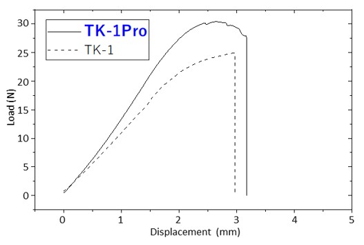
- Improved the mechanical properties of conventional TK-1
- Hardness increased by about 10% from conventional TK-1
- Furthermore, improved toughness contributes to improved machinability during cutting processing
Comparison of Three-Point Bending Characteristics of TK-1Pro and TK-1
Development Material: TK-FS
Achieves low electrical resistivity, high bendability, and a wide hardness range all at the same time.
There was no material in our existing products that could simultaneously achieve the three qualities of high hardness, low electrical resistivity, and high bendability, but we have succeeded in solving this problem with this product, making it possible to use the same material for various types of probe pins. This material can be applied to a wide range of probe pin types, such as the cantilever type and the vertical type for wafer testing (front-end process) probe cards.
Features
- Simultaneously achieves three functions: Vickers hardness of 500 or higher, electrical resistivity of 7.0 µΩ・cm or lower, and repeated bending durability (according to our standards) of 10 times or more.
- Our unique processing technology enables adjustment to a wide range of Vickers hardness (400 to 520).
- Higher elongation (10% to 25%) than TANAKA PRECIOUS METAL TECHNOLOGIES’ existing probe pin materials.
Performance of TK-FS (Comparison with Major Probe Pin Materials)
Vickers Hardness vs Electrical Conductivity
![[Comparison of Material Properties (Hardness/Electrical Conductivity) for Probe Pins]TK-FS and others](https://data.wovn.io/ImageValue/production/688b3c307ffdea2de8055986/en/e40d7e92405496b4c05669f6a35a7eec/wp_content_uploads_sites_images_ex_en_products_images_probe_pins_img_block04_01.jpg)
Elongation at Failure
![[Comparison of Material Properties for Probe Pins (Elongation)] by TK-FS and others](https://data.wovn.io/ImageValue/production/688b3c307ffdea2de8055986/en/d89fd6b1b48426e42ecb91d54ba03cc0/wp_content_uploads_sites_images_ex_en_products_images_probe_pins_img_block04_02.jpg)
Features of TK-FS (High Bending Durability)
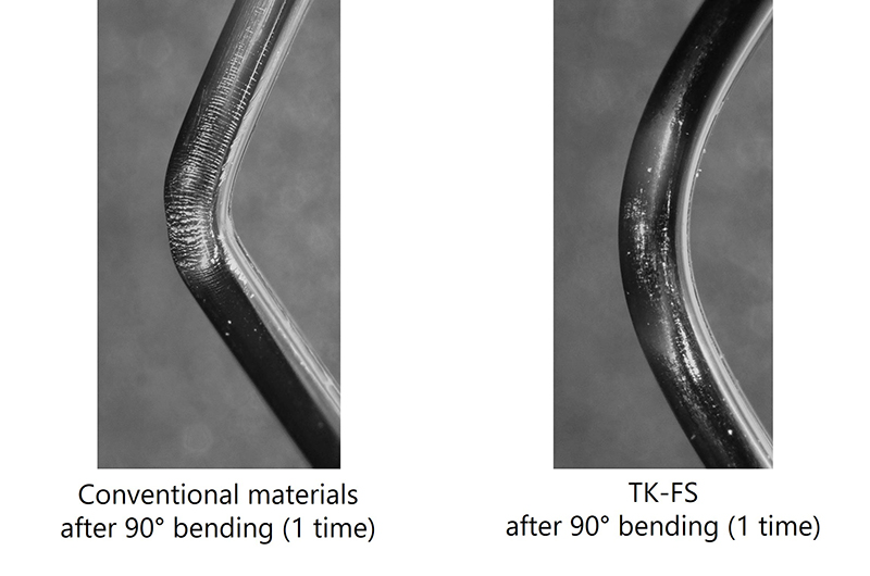
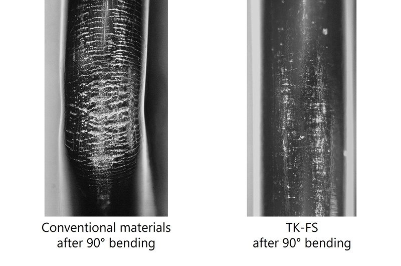
Schematic diagram of repeated 90° Bending Test
Developed material: TK-SK
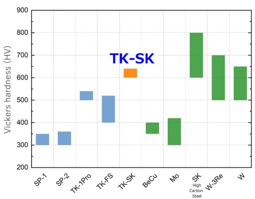
Achieves a hardness of 640 HV as a palladium alloy material.
In semiconductor testing equipment, this product helps reduce deformation of Probe Pins due to wear, contributing to longer service life and lower costs of testing equipment.
Applications
As a palladium alloy for probe pins, TK-SK exhibits maximum hardness of 640HV that makes it suitable for use in test socket applications mainly in the final continuity testing stage (back-end process).
Features
Spring Probe Probe Pins are used as probes in test sockets. During inspection, the tip (plunger) of the Probe Pin deforms due to wear, as friction occurs upon contact with the substrate. In addition, solder material may adhere to the plunger, and it may be necessary to scrape off the solder material for cleaning. The plunger also deforms due to wear during this process.
High-hardness probe pins, like TK-SK, reduce wear-related deformation, leading to longer service life and lower maintenance costs for semiconductor test equipment.
Properties (Reference Values)
| Physical Properties | Reference values |
|---|---|
| Wire diameter range (mm) | 0.50-0.80 |
| Melting point (℃) | 997℃ |
| Density (g/cm3) | 10.52 |
| Vickers hardness (HV) | 640 |
| Electrical resistivity (µΩ·cm) | 16.1 |
| Electrical conductivity (%IACS) | 10.7 |
Comparison of Hardness between Materials for Probe Pins and Non-Precious Metal High Hardness Materials
Development Material: TK-SR
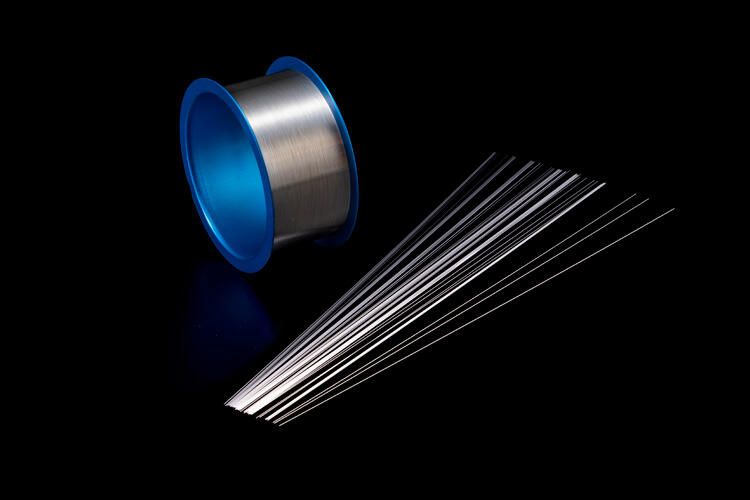
New Rh Probe Pin with High Strength, High Elastic Limit, High Hardness, and High Electrical Conductivity
In semiconductor testing equipment, contributes to the prolonged lifespan and stable performance of probe cards.
Applications
As a Probe Pin material, it is expected to have high and stable performance over a long period of time, and is intended for use in Probe Cards used in wafer testing conducted in the preceding process.
Features
Probe Cards are used for electrical testing of silicon wafers during the front-end process of semiconductor manufacturing, and each card uses several thousand to several tens of thousands of precision Probe Pins. Electrical testing is performed with a slight load applied and is repeated several hundred thousand times, and in some cases, several million times. If even one Probe Pin is deformed or broken, it may be necessary to replace the Probe Pin, and depending on the equipment, it may also be necessary to replace the Probe Card itself. Therefore, Probe Pins are required to have durability that prevents deformation and breakage even under repeated loads.
By using TK-SR with high strength and high elastic limit, the deformation and breakage of Probe Pins can be reduced, and stable performance can be maintained for a long time. In addition, the frequency of component replacement is reduced, contributing to the longer lifespan and lower cost of Probe Cards.
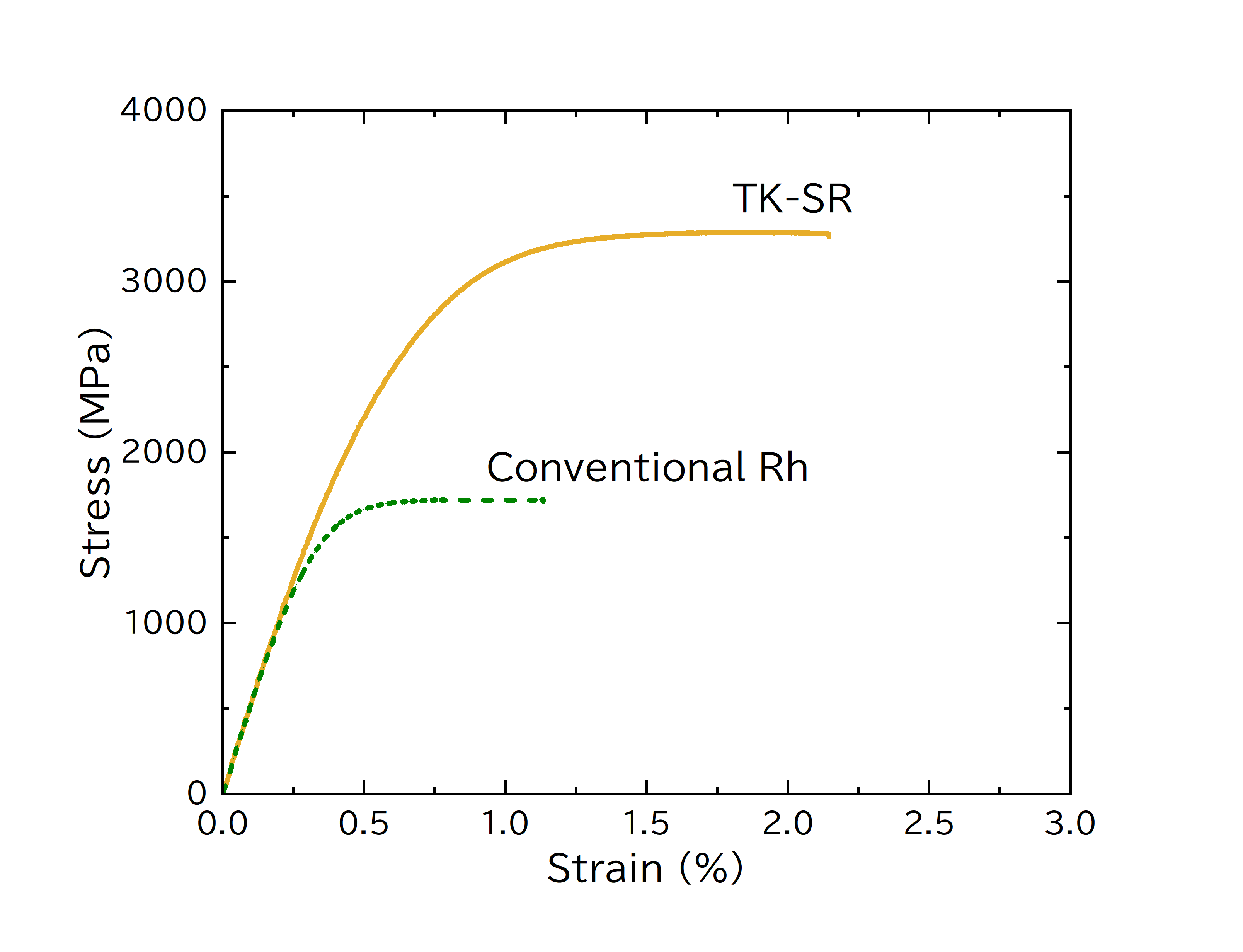
Performance of TK-SR (for reference)
| Characteristics | TK-SR (As Drawn) |
Conventional Rh wire | |
|---|---|---|---|
| Wire diameter [mm] | 0.018 | 0.150 | 0.150 |
| UTS [MPa] | 3860 | 2478 | 1912 |
| Elastic limit [MPa] | 1210 | 1122 | 860 |
| Elongation at break [%] | 2.72 | 2.46 | 1.42 |
| Vickers hardness [HV] | 620 | 543 | 499 |
| Specific resistivity [µΩ・cm] | 6.6 | 6.3 | 5.4 |
Sheet material for vertical probe pins
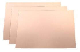
Provides sheets (rolled materials) of various precious metals.
Minimum thickness of 60µm has been achieved, keeping pace with the ongoing miniaturization of electronic components.
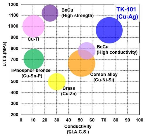
For vertical probe pins, we can provide TK-FS, SP-1, and TK-101 sheet materials.
Characteristics
| TK-FS (Pd-Ag-Cu) |
SP-1 (Pd-Ag-Au-Pt-Cu) |
TK-101 (Cu-Ag) |
||
|---|---|---|---|---|
| Density (g/cm3) | 10.49 | 11.90 | 9.07 | |
| Melting point (℃) | 1,100 | 1,098 | 780 (Solidus) | |
| Electrical resistivity at R.T. (µΩ・cm) |
As-Rolled | – | 25.2 | 2.5 |
| As-Aged | 6* | – | – | |
| Vickers hardness (HV) |
As-Rolled | – | 300 | 330 |
| As-Aged | 400-420* | – | – | |
| Tensile strength (MPa) | 1,200* | 1,100 | 1,000 | |
| Young's modulus (GPa) | 110* | 110 | 105 | |
| 0.2% proof stress/RD (MPa) | 1,150* | – | 900 | |
*TK-FS sheet is under development and the property values are only for reference.
Available sheet sizes
| TK-FS (Pd-Ag-Cu) |
SP-1 (Pd-Ag-Au-Pt-Cu) |
TK-101 (Cu-Ag) |
|
|---|---|---|---|
| Thickness (mm) | 0.06~0.20 | 0.06~0.20 | 0.06~0.20 |
| Width (mm) | ~70 | ~70 | ~70 |
| Length (mm) | ~330 | ~330 | ~330 |
Warp and waviness shall be acceptable for sample products. Conditions can be discussed upon the customer’s requests.
Comparison of Copper Alloy Sheet properties for Probe Pins (Electrical Conductivity/U.T.S. at 20℃)
Related Information


First, please make an Inquiry about the product.
For any questions regarding product specifications, pricing, delivery times, etc., please feel free to Inquiry here.