

Probing the Limits: How Material Innovation Is Meeting the Demands of Fine-Pitch Semiconductor Test
引用元: Semiconductor Digest
日 付: 2026年8月4日
リンク: Probing the Limits: How Material Innovation Is Meeting the Demands of Fine-Pitch Semiconductor Test
著 者: Pete Singer
寄 稿: 布施 健志(田中貴金属工業 製造統括部 伊勢原工場 材料開発セクション マネージャー)
半導体の通電検査(テスト)では、文字どおりの「圧力」と電気的な負荷の双方にさらされながら性能を発揮できる材料が、常に求められてきた。しかし、先端パッケージング、AIアクセラレータのアーキテクチャ、広帯域メモリ(HBM)スタックの要求水準が高まるにつれ、プローブピン材料は従来のアプローチでは物理的な限界に突き当たる領域へと押しやられている。ピッチが50µmを下回り、接触密度が上昇するなかで、業界は単一のパラメータを調整するだけでは解決できない材料課題に直面している。
求められる特性は、よく知られた3つの要素に集約される。酸化膜を突き破り、数百万回にわたる接触サイクルで接触安定性を保つのに十分な「硬さ」。測定対象の信号を歪ませないだけの高い「導電性」。そして、プローブの使用期間中の破断を防ぐ機械的な「延性」である。何十年ものあいだ、プローブカードの設計者やテストエンジニアは、この3つのうち2つを、残る1つを犠牲にして最適化せざるを得なかった。次世代デバイスが要求する寸法において、この3つを同時に成立させること──それが半導体検査における材料イノベーションを駆動してきた中心的な課題である。
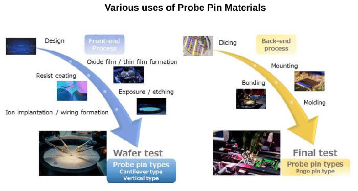
検査工程の全体を支えている。
従来材料が限界に近づいている領域
今日もっとも広く使われているプローブピン材料は、より大きな寸法と低い接触密度が前提だった時代に認定(クオリフィケーション)の実績を積み重ねてきたものである。市場の多くを占めているのはパラジウム合金で、その耐食性と加工性の高さから幅広いプローブ構造に適用でき、長年の使用実績が、半導体メーカーが新材料を量産に導入する前に求める「認定上の安心感」をもたらしている。
しかし、その限界は次第に無視できないものになっている。プローブ用途向けの従来型パラジウム合金は、これまでビッカース硬さでおよそ560 HVが上限とされてきた。加えて、加工硬化させた合金における硬さと延性の従来からのトレードオフが、第二の問題を生む。冷間加工によって高い硬さを得た材料は破断伸びが犠牲になりやすく、場合によっては1〜2%程度まで低下する。その結果、屈曲を伴うプローブ形状や繰り返し荷重下で割れが生じやすくなる。
ロジウムは、これとは異なるトレードオフを抱えている。本来的に弾性率と強度が高いため、高周波用途やファインピッチのバーチカルプローブカードにとって魅力的な材料である。しかし、ロジウムは極めて硬いことから線材加工が難しく、従来の製造では熱間加工に大きく依存してきた。高温下では冷間加工ひずみの蓄積が減ってしまうため、従来工法で製造されたロジウム線は材料が本来もつ弾性と強度を十分に発揮できず、さらに繰り返し荷重下での脆さが、要求の厳しい用途での寿命を制限してきた。
微細化は、この2つの問題をいずれも深刻化させる。従来の伸線プロセスは実用的な下限がおよそ10µmとされ、それを下回ると表面欠陥、寸法ばらつき、真直度の制御、残留応力といった要素が、機械的強度と接触安定性を損なうレベルにまで達する。先端パッケージ検査が現在必要としている18〜25µmの領域では、表面品質の管理が製造上の重要課題となる。
鍵を握るのはプロセス技術
こうした課題に対する材料側の答えは、合金組成だけでなく、プローブ用線材を製造・調質する工程そのものに軸足を置いている。この違いは技術的なニュアンスにとどまらない。プローブピンの性能をどう作り込むか、という考え方の転換を意味している。
従来の合金開発では、硬さは主に加工硬化か単純な析出硬化によって得られてきた。これらのメカニズムは限られた範囲内では予測可能な性能をもたらす一方、硬さ・延性・導電性という三すくみのバランスを取るうえで延性の余地はほとんど残らない。これに対して新しいアプローチは、狙いを定めた合金組成と独自のプロセスシーケンス──綿密に制御された伸線、熱処理条件、塑性変形パラメータ──を組み合わせることで、合金設計だけでは到達できない特性の組み合わせを実現する。

伊勢原工場 材料開発セクション
マネージャー 布施 健志
田中貴金属工業株式会社 製造統括部 伊勢原工場 材料開発セクション マネージャーの布施 健志(理学修士)氏によれば、同社のTK-FS(パラジウム-銀-銅合金)で硬さ・導電性・延性の同時達成を可能にしたブレークスルーは、まさにこの点にあるという。「TK-FSのポイントは、合金組成そのものだけではなく、TK-FS専用に開発した製造プロセスとの組み合わせにあります。伸線、熱処理、塑性変形ひずみといったパラメータを丁寧に最適化しています。その結果、硬さ・導電率・延性を同時に達成できるのです」
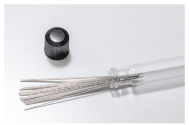
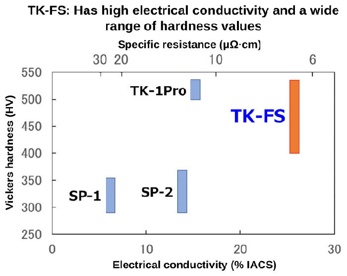
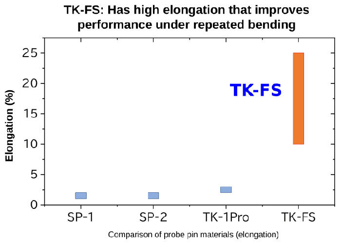
その結果得られたのが、破断伸び10〜25%──従来のプローブピン用合金で一般的な1〜2%と比べて一桁高い水準──を達成しながら、ビッカース硬さ400〜520 HVという広い範囲で調整できる材料である。この「調整できる」という点自体が、プロセス重視のアプローチを反映している。硬さは、冷間加工度と熱処理条件の制御によって、個々の接触要件に合わせて作り込まれる。酸化膜を突き破るために高い硬さが必要なアルミニウムバンプには範囲の上限側で対応し、表面ダメージを最小限に抑えたい金バンプには、より軟らかい設定が求められる。
硬さの上限を押し上げ、ロジウムを捉え直す
従来のパラジウム合金では届かない硬さが求められる用途に対して、業界が目を向けてきたのが時効硬化系の材料である。田中貴金属のTK-SKはその一例で、時効硬化処理後に640 HVへ到達するよう設計された合金でありながら、時効処理前の状態では機械加工性を保っている。従来のパラジウム合金の上限であった約560 HVを大きく超える水準である。
「時効硬化処理の前は、硬さがおよそ380〜400 HVで、プランジャーの機械加工に適した状態です」と布施氏は説明する。「加工後に時効硬化処理を施すことで、最大640 HVの硬さを実現できます」。まず加工し、その後に硬化させる──この順序により、精密なプランジャー形状を従来設備で成形しつつ、最終部品としてはパラジウム系ではこれまで実現が難しかった硬さに到達させることができる。
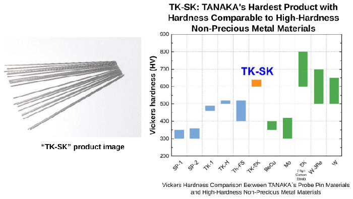
タングステンやW-3Reといった非貴金属系の高硬度材料と同じ領域に位置づける。
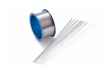
ロジウムの課題には、根本的に異なるアプローチが取られた。材料が本来もつ機械的特性を発揮できるよう、製造プロセスそのものを再設計するというものである。「従来の製法は熱間加工に大きく依存してきました」と布施氏は指摘する。「高温では冷間加工ひずみの蓄積が減ってしまうため、材料が本来もつ弾性と強度を十分に引き出せていませんでした」。ひずみの蓄積を最大化するようプロセスを再設計することで、TK-SRは、ロジウムの物性から期待されながら従来工法では引き出せなかった高い弾性を実現している。
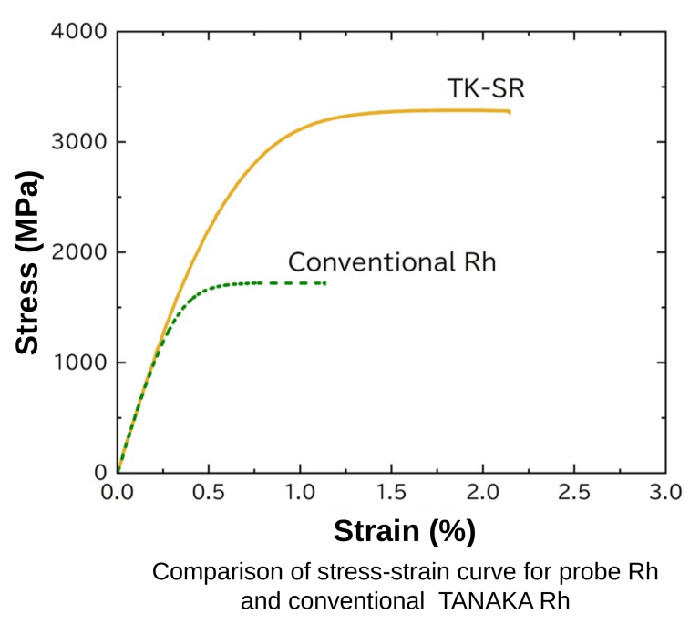
同一ひずみにおける応力は、田中貴金属の従来Rh材のおよそ2倍に達する。
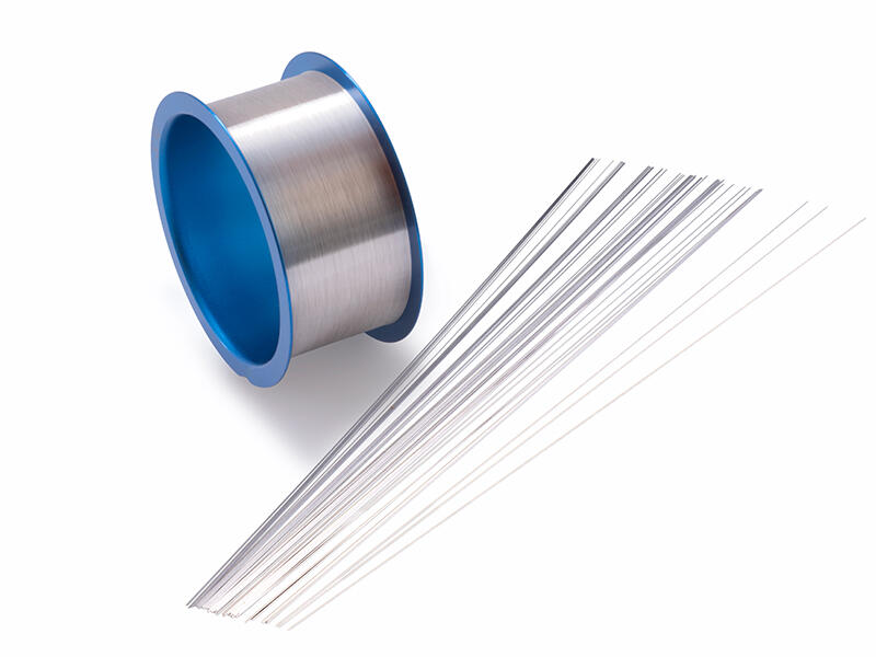
プロセスの変更は、ロジウム線材を細径化する際の障壁となっていた表面品質の問題にも効いた。従来のロジウム線材は、伸線中に表面欠陥に起因する断線が頻発していた。田中貴金属が見直したプロセスによって表面品質が向上した結果、18µmのロジウム線材を安定して生産できるようになった。これは従来は安定的な実現が難しかった径であり、先端パッケージ検査用途で現在求められる範囲に入るものである。
材料選定をどう進めるか
プローブピン材料の選択肢が広がったことで、プローブカード設計者やテストエンジニアには実務上の選定という課題が生じている。布施氏は、3つの判断軸からなるフレームワークを示す。検査用途(ファイナルテスト用ソケットか、ウエハーテスト用プローブカードか)、プローブ構造(カンチレバー、バーチカル、ポゴピン)、そして最優先の性能要件(導電率、耐摩耗性、曲げ性、コスト、実績ある信頼性)である。
ファイナルテスト用ソケットでは、コストパフォーマンスのバランス、あるいは精密な耐摩耗性のいずれかにトレードオフが寄る。ウエハーテスト用プローブカードでは、接触安定性とアーキテクチャとの適合性が中心となり、プローブ構造に応じてロジウム系やイリジウム系まで候補が広がる。カンチレバータイプは、設置時や動作時に大きな曲げを受けるため、とりわけ延性の高い材料が有利である。一方、バーチカルタイプの用途では、硬さと弾性回復により重きが置かれる。
なお、既存材料のなかには、より新しい選択肢に対する技術的な優位性というよりも、長い認定実績を根拠に量産で使われ続けているものもある。再認定に相応の時間とコストがかかる業界においては、現実的な判断といえるだろう。ただし、ピッチの微細化が進み、新しい接触部の金属種が増えるにつれて、この計算は変わりつつある。既存材料と新材料の性能差は、移行に伴う投資を正当化できるほど大きくなってきているのである。
寸法のスケーリング──次に立ちはだかる制約
硬さの上限、導電率の下限、幾何学的な微細化──現在の材料上の制約のうち、どれが最初に効いてくる限界となるかを問われた布施氏は、寸法のスケーリングを挙げる。「現時点では、従来の伸線プロセスの実用的な下限はおよそ10µmです。この寸法域では、微視的な欠陥、寸法ばらつき、真直度、残留応力が、機械的強度と接触安定性に大きく影響します」
ここから示唆されるのは、硬さと導電率の向上は依然として必要ではあるものの、次世代デバイスが求める幾何学的な要求に、そのスピードが追い抜かれかねないということである。10µmを下回るピッチのパッドに接触できるプローブ構造には、伸線の枠を超えた製造上のブレークスルー──プローブの形成方法、表面の制御、残留応力の管理に関する新たなアプローチ──が必要になる。
チップレット、広帯域メモリ(HBM)スタック、ファンアウト型ウエハーレベルパッケージといった先端パッケージのアーキテクチャは、接触密度の要求を高めると同時に、基板側の金属種の幅も広げている。テストエンジニアは、旧来世代を特徴づけてきたアルミニウムや金に加えて、銅ピラー、スズ-銀はんだキャップ、各種の金属間化合物表面といった接触材料に向き合わなければならない。この金属種の多様性は、プローブ材料の選定と表面の調質に、さらなる要求を突きつけている。
TCO(総所有コスト)とサーキュラーエコノミー
プローブピン材料は、パラジウムやロジウムをはじめとする白金族金属(PGM)を相当量消費する。現在のPGM価格を前提とすると、プローブカードに含まれる貴金属は無視できない資本投下となる。ところが、それが初期材料コストの観点で分析されることは多い一方、プローブの使用期間全体を通じた総所有コスト(TCO)の観点で語られることはあまり多くない。
より包括的なTCO分析には、使用寿命と交換頻度、接触抵抗のドリフトが歩留まりに与える影響、プローブ交換に伴う装置のダウンタイム、そして寿命到達時に回収できる貴金属の残存価値が含まれる。田中貴金属は貴金属の回収・精製・リサイクルを一貫して手がけており、顧客は使用済みプローブピンや製造スクラップを返却して処理を委託することで、残存するPGM価値を回収し、新規材料コストの一部を相殺できる。
「TCOを評価する際には、初期の材料コストだけでなく、使用寿命の延長と交換頻度の低減、歩留まりの改善、装置ダウンタイムの削減、そして貴金属の回収価値もあわせて考慮すべきです」と布施氏は説明する。「これらの要素を総合することで、その材料がもつ経済的価値をより正確に評価することができます」
TCOの観点にとどまらず、サーキュラーエコノミーは貴金属の資源マネジメントにおいてますます重要な論点になっている。田中貴金属は、貴金属の調達、精製、材料製造、リサイクルをワンストップで担う体制を備え、貴金属の持続可能かつ効率的な利用を促す循環型サプライチェーンを支えている。これにより、貴金属の調達に伴うCO2排出量全体の削減に寄与しつつ、貴金属材料の安定供給を下支えする。
業界全体で向き合う課題
半導体検査の要求水準の推移を見れば、プローブピン材料に漸進的な改良の余地はほとんど残されていない。ピッチの微細化、接触密度の上昇、基板側の金属種の多様化、そして先端ノードで厳格化する信号品質(シグナルインテグリティ)の要件が重なり、10年前であれば実現困難だった材料とプロセスへと、この分野を押し進めている。
近年の材料開発から浮かび上がるパターンは一貫している。最も大きな性能向上をもたらしているのは合金組成だけではなく、狙いを定めた組成と独自のプロセスシーケンスの組み合わせであり、それによって従来の製造では到達できない特性の組み合わせが可能になる、ということである。パラジウム合金における硬さ・延性・導電性の同時達成であれ、時効硬化系における超高硬度と機械加工性の両立であれ、プロセス再設計によるロジウム本来の機械的特性の実現であれ──進歩は「どう作るか」と切り離すことができない。
次の課題である10µmを下回る領域での安定したプローブ接触は、さらなるプロセス上のブレークスルーを、そして場合によってはプローブ形成そのものへの新しいアプローチを必要とするだろう。半導体検査業界は、デバイスのスケーリングに歩調を合わせる手段を一貫して見出してきた。いま問われているのは、すでに開発が進んでいるデバイスに間に合う速さで、材料と製造のツールボックスを広げられるかどうかである。
布施 健志(理学修士)氏は、田中貴金属工業株式会社 製造統括部 伊勢原工場 材料開発セクション マネージャーとして、TK-FS、TK-SK、TK-SRの各合金シリーズからなる同社のプローブピン材料を統括している。これらの材料は、貴金属のリサイクル・精製を一貫して担う体制に支えられている。
関連リンク

【サイドバー】先端パッケージにおけるプローブアクセスの問題
先端パッケージングは、半導体デバイスを「検査する」という行為の意味を書き換えた。チップレットアーキテクチャ、2.5D/3Dスタッキング、広帯域メモリの統合が進んだ結果、いくつかの重要な点でプロービング工程に本質的に不利なパッケージ構造が生まれている。それはプローブ材料が不十分だからではなく、アクセスの幾何学そのものが変わったからである。
Known Good Die(良品ダイ)。スタック型やチップレット型のパッケージでは、組み立て後に見つかった不良ダイが1つあるだけで、ユニット全体──場合によっては数百ドル相当のHBMスタックを含む──が台無しになる。したがって、組み立て前にKGD(Known Good Die)の状態を確保しようとする経済的な圧力は非常に強く、その役割はウエハーテストが担うことになる。しかし、信頼できるKGDスクリーニングに必要なプローブ条件は、ファイナルテストのそれとますます区別がつかなくなっている。ファインピッチ、多様なバンプ金属種、そしてプローブピン材料を限界まで酷使するサイクル数である。
埋め込み配線。ダイが積層されると、その間をつなぐ配線──TSV、マイクロバンプ、ハイブリッドボンディング界面──には、外部プローブから物理的にアクセスできない。構造テストのカバレッジは、設計時に組み込まれたBIST(ビルトインセルフテスト)回路とDFT(テスト容易化設計)構造に全面的に依存することになる。つまり、テスト戦略とパッケージのアーキテクチャは同時に設計されなければならない。内部配線へのDFTアクセスを備えないパッケージは、プローブ側のハードウェアがどれだけ高性能であっても、十分にスクリーニングすることができないのである。
反り(ワーページ)。ヘテロジニアスなパッケージは、熱膨張係数の異なる材料──シリコンダイ、有機基板、インターポーザ、アンダーフィル、モールド樹脂──で構成され、それぞれ膨張の度合いが異なる。動作温度でのウエハーテストでは、接触アレイ全体で数十µmのばらつきをもつ反りプロファイルに遭遇することがある。プローブカードのコンプライアンス、オーバードライブの管理、平坦度の制御は、いずれも温度によって動く対象を前提としなければならない。モノリシックなデバイスの検査では、この規模で生じることのなかった課題である。
接触部の金属種の多様化。1つの先端パッケージのなかで、銅ピラー、スズ-銀はんだキャップ、アルミニウムRDLパッド、ニッケル/金UBM表面が同一の接触アレイ内に混在することがある。金属種ごとに硬さも、酸化膜の生成挙動も、接触ダメージへの許容度も異なる。アルミニウム上で強く酸化膜を突き破るよう最適化されたプローブピンは、より軟らかいはんだ表面に対しては許容できないダメージを与えかねない。この金属種の多様性が、テストエンジニアをマルチゾーン型のプローブカード設計と、本記事で述べたような調整可能な特性プロファイルをもつピン材料へと向かわせている。
並列測定と熱負荷。AIアクセラレータや高性能コンピューティング向けパッケージは、I/O数が多く、消費電力も大きくなる。フルの動作負荷で検査するには、ファインピッチで数百から数千のパッドに同時接触しながら、300W以上を消費するデバイスの発熱を管理しなければならない。検査中に発生する熱は、プローブカードの機械的な状態と、デバイスの反りプロファイルを変化させる。従来は二次的な検討事項だった治具の熱管理は、いまや先端パッケージのプロービングにおける一次的な設計パラメータである。
結果として生まれているのは、プローブピン材料の特性を、単一の安定した接触条件ではなく、動的なシステムに向けて最適化しなければならない検査環境である。多様な金属種、温度とともに変化する機械的荷重、そして組み立て後の不良流出コストによって決まるサイクル数の要求。プローブピンにおける材料イノベーションは、先端パッケージ検査を成功させるための必要条件ではあるが、それだけでは十分ではない。プローブアクセスの課題は、最終的にはシステムの問題であり、プローブ材料、カード設計、治具エンジニアリング、そしてデバイス側のDFTが並行して進歩することを求めている。
【著者】 Pete Singer
【プロフィール】40年以上の出版経験。2019年に発行人のKerry Hoffman氏とともに Semiconductor Digest とGold Flag Media社を共同設立。
それ以前は Semiconductor International に25年以上、Solid State Technology に11年在籍。
【引用元】
Probing the Limits: How Material Innovation Is Meeting the Demands of Fine-Pitch Semiconductor Test - Semiconductor Digest
Source: Semiconductor Digest
Date: August 4, 2026
Link: Probing the Limits: How Material Innovation Is Meeting the Demands of Fine-Pitch Semiconductor Test
Author: Pete Singer
Contribution: Takeshi Fuse (Manager, Materials Development Section, Manufacturing Management Dept., TANAKA PRECIOUS METAL TECHNOLOGIES Co., Ltd.)
Semiconductor test has always demanded materials that perform under pressure -- literally and electrically. But the escalating requirements of advanced packaging, AI accelerator architectures and high-bandwidth memory stacks are pushing probe pin materials into territory where conventional approaches reach hard physical limits. As pitches shrink below 50 µm and contact densities climb, the industry is confronting a materials challenge that no single dial can solve.
The demands converge on a familiar triad: hardness sufficient to penetrate oxide layers and maintain contact stability over millions of cycles; electrical conductivity high enough not to distort the signals being measured; and mechanical ductility that prevents fracture during the probe's working life. For decades, probe card designers and test engineers have been forced to optimize two of these properties at the expense of the third. Getting all three simultaneously -- at the dimensions required by next-generation devices -- has been the central challenge driving materials innovation in semiconductor test.
Where Conventional Materials are Reaching Their Limits
The probe pin materials in widest use today trace their qualification histories back to an era of larger feature geometries and lower contact densities. Palladium alloys dominate much of the market: their corrosion resistance and workability make them practical for a wide range of probe structures, and their long track record provides the qualification confidence that semiconductor manufacturers require before introducing new materials into production.
The limitations, however, are becoming more consequential. Conventional palladium alloys for probe applications have historically topped out at around 560 HV (Vickers hardness). Meanwhile, the conventional relationship between hardness and ductility in work-hardened alloys creates a second problem: materials that achieve higher hardness through cold working typically sacrifice elongation at failure, sometimes to as little as 1-2%, making them susceptible to cracking in bent probe geometries or under repeated loading.
Rhodium presents a different set of tradeoffs. Its inherently high elastic modulus and strength make it attractive for high-frequency applications and fine-pitch vertical probe cards. But rhodium's extreme hardness has historically made wire processing difficult, and conventional manufacturing has relied heavily on hot-working techniques. Because elevated temperatures reduce cold-work strain accumulation, conventionally processed rhodium wire cannot fully realize the material's intrinsic elasticity and strength -- and brittleness under repeated loading has limited service life in demanding applications.
Miniaturization compounds both issues. Conventional wire-drawing processes reach a practical lower limit at approximately 10 µm, below which surface defects, dimensional variation, straightness control, and residual stress become severe enough to compromise mechanical strength and contact stability. At 18-25 µm -- the range now required by advanced packaging inspection -- surface quality control becomes a critical manufacturing challenge.
Process Technology as the Key Variable
The materials response to these challenges has centered not just on alloy composition, but on the manufacturing processes used to produce and condition probe wire. This distinction is more than technical nuance -- it represents a shift in how probe pin performance is engineered.
In conventional alloy development, hardness is achieved primarily through work hardening or simple precipitation hardening. These mechanisms deliver predictable performance within a limited range but offer little ductility in balancing the hardness-ductility-conductivity triad. The emerging approach combines tailored alloy compositions with proprietary process sequences -- carefully controlled wire drawing, heat treatment schedules, and plastic deformation parameters -- to achieve property combinations that alloy design alone cannot reach.
According to Takeshi Fuse, M.S., Section Manager, Materials Development Section, Manufacturing Management Dept at TANAKA PRECIOUS METAL TECHNOLOGIES Co., Ltd., the breakthrough enabling simultaneous hardness, conductivity, and ductility in their TK-FS palladium-silver-copper alloy lies precisely here: "The key point of TK-FS is not only the alloy composition itself, but also the combination of a dedicated manufacturing process developed specifically for TK-FS. Parameters such as wire drawing, heat treatment, and plastic deformation strain are carefully optimized. As a result, hardness, electrical conductivity, and ductility can be achieved simultaneously."
The result is a material that achieves 10-25% elongation at failure -- an order of magnitude above the 1-2% typical of conventional probe pin alloys -- while remaining adjustable across a wide Vickers hardness range of 400-520 HV. That adjustability itself reflects the process-centric approach: hardness is tuned by controlling cold work degree and heat treatment conditions to match specific contact requirements. Aluminum bumps, which require higher hardness to penetrate the oxide layer, can be addressed at the upper end of the range; gold bumps, where surface damage must be minimized, call for softer settings.
Pushing the Hardness Ceiling and Reimagining Rhodium
For applications demanding hardness beyond what conventional palladium alloys can deliver, the industry has looked toward age-hardenable systems. TANAKA's TK-SK material illustrates the approach: an alloy designed to reach 640 HV after age hardening -- a significant step beyond the ~560 HV ceiling of previous palladium alloys -- while retaining machinability in the pre-aged state.
"Prior to age-hardening treatment, the material exhibits a hardness of approximately 380-400 HV, which is suitable for plunger machining," explains Fuse. "After machining, age hardening is applied, enabling the material to achieve a maximum hardness of 640 HV." This sequence -- machine first, then harden -- allows precision plunger geometries to be achieved using conventional equipment, while the final component reaches hardness levels that were previously impractical in palladium-based systems.
The rhodium challenge has been addressed through a fundamentally different intervention: redesigning the manufacturing process to allow the material to realize its inherent mechanical properties. "Conventional manufacturing methods have relied heavily on hot-working processes," Fuse notes. "Because elevated temperatures reduce the accumulation of cold-work strain, the material has been unable to fully realize its intrinsic elasticity and strength." By redesigning the process to maximize strain accumulation, TK-SR achieves the high elasticity that rhodium's material properties imply but that conventional processing has not been able to unlock.
The process change also addresses the surface quality problems that had limited rhodium wire to larger diameters. Conventional rhodium wire frequently suffered wire breakage caused by surface defects during drawing. The improved surface quality achieved through TANAKA's revised process has enabled consistent production of 18 µm rhodium wire -- a diameter previously difficult to achieve reliably and one that falls within the range now required for advanced packaging inspection applications.
Navigating Material Selection
The expanding palette of probe pin materials creates a practical selection challenge for probe card designers and test engineers. Mr. Fuse describes a framework built around three decision variables: test application (final test socket or wafer probe card), probe structure (cantilever, vertical, or pogo pin), and the primary performance requirement (electrical conductivity, wear resistance, bendability, cost, or established reliability).
For final test sockets, the tradeoffs lean toward cost-performance balance or precision wear resistance. For wafer probe cards, contact stability and architecture compatibility become central, and the candidate set expands to include rhodium-based and iridium-based materials depending on probe structure. Cantilever probes particularly benefit from materials with high ductility, since the probe undergoes significant bending during installation and operation; vertical probe applications place greater emphasis on hardness and elastic recovery.
It is worth noting that some legacy materials remain in production service largely on the basis of their long qualification history rather than technical superiority to newer alternatives -- a practical reality in an industry where requalification carries significant time and cost. As pitches continue to shrink and new contact metallurgies proliferate, the qualification calculus is shifting: the performance gap between legacy and newer materials is becoming large enough to justify the transition investment.
Dimensional Scaling: The Binding Constraint Ahead
Asked which of the current material constraints -- hardness ceiling, conductivity floor, or geometric miniaturization -- is likely to become the binding limit first, Fuse identifies dimensional scaling. "At present, approximately 10 µm represents a practical lower limit for conventional wire-drawing processes. At these dimensions, microscopic defects, dimensional variation, straightness, and residual stress significantly affect mechanical strength and contact stability."
The implication is that advances in hardness and conductivity, while still needed, may be outpaced by the geometric demands of next-generation devices. Probe structures capable of contacting pads at sub-10 µm pitches will require manufacturing breakthroughs that go beyond wire drawing: new approaches to probe formation, surface control, and residual stress management.
Advanced packaging architectures -- chiplets, high-bandwidth memory stacks, fan-out wafer-level packages -- are simultaneously raising the contact density requirements and introducing a broader range of substrate metallurgies. Test engineers must now contend with contact materials that include copper pillars, tin-silver solder caps, and various intermetallic surfaces alongside the aluminum and gold that defined earlier generations. This metallurgical diversity places additional demands on probe material selection and surface conditioning.
Total Cost of Ownership and the Circular Economy
Probe pin materials consume palladium, rhodium, and other platinum group metals (PGMs) at scale. At current PGM prices, the precious metal content of a probe card represents a significant capital commitment -- one that is often analyzed in terms of initial material cost but less often in terms of total cost of ownership (TCO) over the probe's working life.
A more complete TCO analysis incorporates service life and replacement frequency, yield impact from contact resistance drift, equipment downtime associated with probe changes, and the residual precious metal value recoverable at end of life. TANAKA's integrated precious-metal recovery, refining, and recycling capabilities allow customers to return used probe pins and manufacturing scrap for processing, recovering the residual PGM value and partially offsetting new material costs.
"When evaluating TCO, consideration should be given not only to initial material cost, but also to extended service life and reduced replacement frequency, yield improvement, reduced equipment downtime, and recovery value of precious metals," Fuse explains. "These factors together provide a more accurate assessment of the total economic value of the material."
Beyond TCO considerations, the circular economy is becoming an increasingly important aspect of precious metal resource management. TANAKA's one-stop capabilities in precious metal procurement, refining, materials manufacturing, and recycling support a circular supply chain that promotes the sustainable and efficient use of precious metals, helping reduce the overall carbon dioxide footprint associated with precious metal sourcing while supporting a stable supply of precious metal materials.
An Industry-Wide Challenge
The trajectory of semiconductor test requirements leaves little room for incremental improvement in probe pin materials. The combination of finer pitches, higher contact densities, diverse substrate metallurgies, and tightening signal integrity requirements at advanced nodes is pushing the field toward materials and processes that would have been impractical a decade ago.
The pattern emerging from recent materials development is consistent: the most significant performance gains are coming not from alloy composition alone, but from the combination of tailored compositions with proprietary process sequences that enable property combinations conventional manufacturing cannot achieve. Whether that means simultaneous hardness, ductility, and conductivity in a palladium alloy, ultra-high hardness with retained machinability in an age-hardenable system, or the realization of rhodium's inherent mechanical properties through process redesign -- the advance is inseparable from how the material is made.
The next challenge -- reliable probe contact below 10 µm -- will likely demand further process breakthroughs, and potentially new approaches to probe formation altogether. The semiconductor test industry has consistently found ways to keep pace with device scaling. The question now is whether the materials and manufacturing toolbox can be extended quickly enough to meet devices that are already in development.
Takeshi Fuse, M.S., is Section Manager, Materials Development Section, Manufacturing Management Department at TANAKA PRECIOUS METAL TECHNOLOGIES Co., Ltd., overseeing TANAKA's probe pin materials include the TK-FS, TK-SK, and TK-SR alloy families, supported by integrated precious-metal recycling and refining capabilities.
Additional links
Sidebar: The Probe Access Problem in Advanced Packages
Advanced packaging has redefined what it means to test a semiconductor device. The push toward chiplet architectures, 2.5D/3D stacking, and high-bandwidth memory integration has produced package structures that are, in important ways, fundamentally hostile to the probing process -- not because probe materials are inadequate, but because the geometry of access itself has changed.
Known Good Die. In a stacked or chiplet package, a defective die discovered after assembly contaminates the entire unit -- potentially including HBM stacks worth hundreds of dollars. The economic pressure to achieve known good die (KGD) status before assembly is therefore intense, and it falls on wafer probe to deliver it. But the probe conditions required for reliable KGD screening are increasingly indistinguishable from those of final test: fine pitch, diverse bump metallurgies, and cycle counts that stress probe pin materials to their limits.
Buried Interconnects. Once dies are stacked, the interconnects between them -- TSVs, microbumps, hybrid bonding interfaces -- are physically inaccessible to external probes. Structural test coverage relies entirely on built-in self-test (BIST) circuits and design-for-testability (DFT) structures embedded at design time. This means test strategy and package architecture must be co-designed: a package that doesn't provide DFT access to its internal interconnects cannot be adequately screened regardless of how capable the probe hardware is.
Warpage. Heterogeneous packages are built from materials with mismatched coefficients of thermal expansion -- silicon dies, organic substrates, interposers, underfill, and molding compound all expand at different rates. Wafer probe at functional temperatures can encounter warpage profiles that vary by tens of microns across the contact array. Probe card compliance, overdrive management, and planarity control must all account for a target that is moving as a function of temperature -- a challenge that monolithic device test never posed at this scale.
Contact Metallurgy Diversity. A single advanced package may present copper pillars, tin-silver solder caps, aluminum RDL pads, and nickel/gold UBM surfaces within the same contact array. Each metallurgy has different hardness, oxide formation behavior, and tolerance for contact damage. Probe pins optimized for aggressive oxide penetration on aluminum may cause unacceptable damage on softer solder surfaces. This metallurgical diversity is pushing test engineers toward multi-zone probe card designs and pin materials with the adjustable property profiles described in this article.
Parallelism and Thermal Load. AI accelerators and high-performance compute packages have high I/O counts and high power dissipation. Testing them at full functional load requires simultaneous contact with hundreds or thousands of pads at fine pitch, while managing the thermal output of a device dissipating 300W or more. Heat generated during test alters the mechanical state of the probe card and the warpage profile of the device. Fixture thermal management -- traditionally a secondary concern -- is now a first-order design parameter for advanced package probe.
The cumulative effect is a test environment in which probe pin material properties must be optimized not for a single stable contact condition, but for a dynamic system: diverse metallurgies, mechanical loads that shift with temperature, and cycle count requirements driven by the cost of post-assembly defect escapes. Material innovation in probe pins is a necessary condition for success in advanced package test -- but it is not sufficient on its own. The probe access challenge is ultimately a systems problem, requiring probe materials, card design, fixture engineering, and device DFT to advance in parallel.
[Author] Pete Singer
[Profile] Pete has over 40 years of publishing experience. He co-founded Semiconductor Digest and the Gold Flag Media company with publisher Kerry Hoffman in 2019. Previously, he spent over 25 years at Semiconductor International and 11 years at Solid State Technology.
[Source]
Probing the Limits: How Material Innovation Is Meeting the Demands of Fine-Pitch Semiconductor Test - Semiconductor Digest
이 기사는 어땠어?
참고가 된 분은, 공유를 부탁합니다.


