

構想から実行へ:持続可能な半導体エコシステムの構築を目指すインド
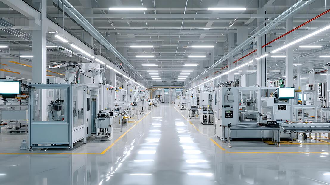
引用元: Dataquest
日 付: 2026年7月20日
リンク: From ambition to execution: India's path towards sustainable semiconductor ecosystem
寄 稿: Das Subhabrata(株式会社田中貴金属グループ 科学広報担当)
半導体製造の発展を左右するのは、製造工場への投資による生産能力の拡大だけではない。高い精度や歩留まり、厳格なプロセス管理も同様に重要である。
2021年末、電子機器需要の拡大や輸入への依存、サプライチェーンの脆弱性が顕在化するなか、インドでは大胆な対応が求められていた。こうした状況を受け、インド政府は「インド半導体ミッション(India Semiconductor Mission:ISM)」を立ち上げた。
その後、インドの半導体産業は、世界的な製造拠点となることを目指して着実に発展を続けている。その推進策の一つが、インド国内に半導体ウエハー製造工場(ファブ)を設置する企業に対する、最大50%の財政支援である。こうした取り組みを背景に、インドの半導体市場は2030年までに1,000億~1,100億米ドル規模に達すると予測されている(インド政府報道情報局〔PIB〕)。
さらに近年では、この取り組みを「ISM 2.0」へと拡充する動きが進んでいる。2026~2027年度には、100億ルピー(約1億600万米ドル)の追加予算が計上され、半導体製造能力の拡大に加えて、半導体材料、製造装置、研究開発、サプライチェーンの整備にも、これまで以上に重点が置かれている。
しかし、半導体製造の競争力を決定づけるのは、製造工場や、組立・検査・マーキング・梱包を担うATMP施設への投資によって生産能力を拡大することだけではない。高い製造精度や歩留まりを確保し、厳格なプロセス管理を徹底することも、同様に重要である。
本記事はDataquestに掲載されたものであり、詳細は以下より確認可能である。
続きを見る (Dataquest)
Source: Dataquest
Date: July 20, 2026
Link: From ambition to execution: India's path towards sustainable semiconductor ecosystem
By : Subhabrata Das, Scientific Communicator, TANAKA PRECIOUS METAL GROUP Co., Ltd.
Semiconductor manufacturing is defined as much by precision, yield, and process discipline as it is by the growth in installed capacity from investments in fabrication plants
At the tail-end of 2021, rising electronics demand, import dependence, and supply chain vulnerabilities, required bold responses and the government of India launched the India Semiconductor Mission (ISM).
Since then, the Indian semiconductor ecosystem has been on a steady path to becoming a global manufacturing hub through incentives such as fiscal support of up to 50% for setting up semiconductor wafer fabrication units (fabs) in India. The result is a projected market value of USD 100-110 billion by 2030 (PIB).
More recently, the initiative is set for expansion as ISM 2.0, which includes a INR 1,000 crore ($106 million) boost for the 2026-2027 fiscal year, places greater emphasis on semiconductor materials, equipment, research, and supply chain development alongside fabrication capacity expansion.
However, semiconductor manufacturing is defined as much by precision, yield, and process discipline as it is by the growth in installed capacity from investments in fabrication plants, and Assembly, Testing, Marking, and Packing (ATMP) facilities.
This article was published in Dataquest, and further details can be found below.
Read more (Dataquest)
この記事はどうでしたか
参考になった方は、シェアをお願いします。


